MEMS Engineering & Materials' bonded products include:
- SOI wafer with uniformity of +/-0.1μ
- Multi-device layer SOI wafer
- New engineering substrate (such as GaAs/Si, glass/Glass)
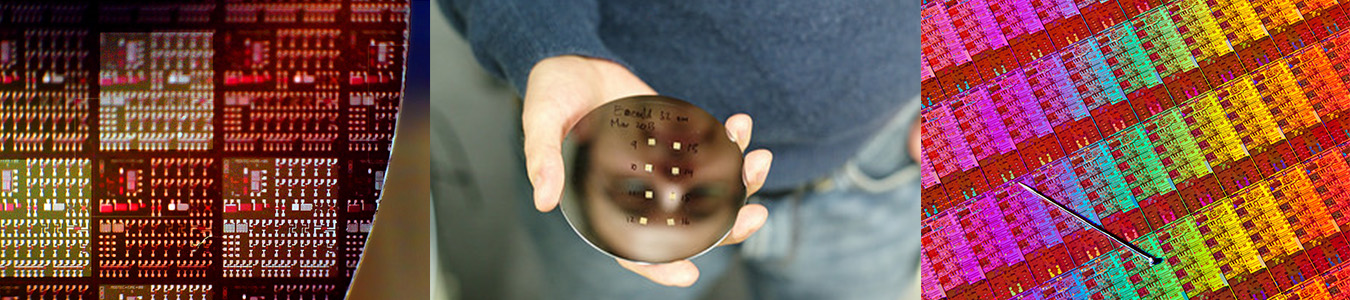
Ultra flat SOI: world’s most uniform SOI wafers (+/-0.1 micro)
We have made a major technological breakthrough to make Ultraflat SOI wafers. Through this new technology, we are able to make SOI wafers as uniform as +/-0.1 micro with any resistivity, orientation, and thickness, greatly surpassing the limitations of Smart Cut technology. We can now produce a 0.5µm device layer with heavy doping, and can provide SOI wafer with device layer thickness of 1.0±0.10µm. Traditionally, this could only be done through a complicated Smart Cut plus EPI growth process, which would be significantly more expensive.
Our SOI wafers are widely used in the following areas:
- 1. MEMS
- 2. Smart sensors
- 3. Power devices
- 4.Semiconductor
Silicon On Glass
Silicon on glass wafers are fabricated by anodic bonding which relies on charge migration to create bonded wafers. By applying certain negative potential to the glass at elevated temperature, sodium ions in the glass are driven to negative electrode to create a space charge at the glass-silicon interface. This space charge gives a strong electrostatic forces between the silicon and glass that holds both pieces. Oxygen from glass simultaneously transfers to the interface of glass and silicon to form silicon oxide, which creates a permanent bonding.
Our silicon on glass wafers can be used in the following applications:
- 1. Pressure sensors
- 2. Solar cell
- 3. Packaging
- 4. Optical components
What We Offer
- 1. Flexibility, thickness of wafer and oxide, resistivity of wafer
- 2. Skilled staff that will work with you to design and customize SOI for robust MEMS processes
MEMS Engineering & Material has the capability to fabricate other bonded structures, such as Glass to glass, SOS (silicon on Sapphire), GaAs/Si, InP/Si for application in MEMS and semiconductor industries. We also like to establish partnerships with customers to develop customized bonded structures bashing on our bonding technologies.