
SOI wafers, bonded substrates and silicon, made and stocked in Sunnyvale.
We fabricate SOI wafers with ultra-uniform device layers and ultra-low stress, build custom bonded structures, and keep a working inventory of SOI, CZ and float zone wafers.
- Device layer
- 100 nm – 200 µm
- Buried oxide
- up to 15 µm
- Handle wafer
- from 100 µm
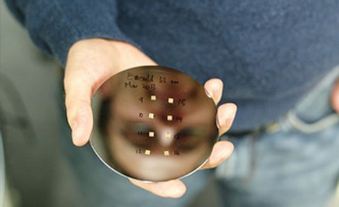
device layer uniformity, with any resistivity, orientation and thickness
Ultra-flat SOI, without Smart Cut
We have made a major technological breakthrough in making ultra-flat SOI wafers: as uniform as ±0.1 µm with any resistivity, orientation and thickness, greatly surpassing the limitations of Smart Cut technology.
We now produce 0.5 µm device layers with heavy doping, and SOI wafers with a 1.0 ± 0.10 µm device layer. Traditionally this needed a complicated Smart Cut plus epi growth process, at significantly higher cost.
SOI wafer specifications and stock →What we make
Buy from inventory when a lot fits. Everything else is built to your specification.
SOI wafers
Bonded SOI with device layers from 100 nm to 200 µm, thermal or CVD buried oxide, and handles as thin as 100 µm.
Silicon & FZ wafers
CZ and float zone silicon, plus silicon germanium, sapphire, compound, epitaxial, film-coated, glass and quartz wafers.
Advanced substrates
Low-temperature bonding for silicon on glass, sapphire and quartz; III-V, GaN and PZT on silicon; GaN on diamond. Debondable SOI, ultra-thin and ultra-flat silicon.
Wafer foundry service
Thin films, photolithography, plating, etching, bonding, dicing, grinding and CMP, from single steps to prototype runs. Interposers and through-via silicon and glass wafers.
In stock now
Every lot listed is on our shelves. Priced wafers can be requested online; SOI lots are quoted with your request.
Talk to the people who make the wafers.
- Telephone
- 408-921-6679
- Address
- 1159 Sonora Ct, Sunnyvale, CA 94086